
Finland’s contribution to the European semiconductor pilot line is strengthening its position in the European chip industry and creating new growth opportunities for companies.
The chip industry is critical to Finland’s long-term competitiveness, as it requires access to the latest technology and expertise to develop, manufacture and exploit critical technologies. Finland brings to the European chip industry solid expertise and experience in specialized microelectronics such as radio frequency (RF), microelectromechanical systems (MEMS), integrated photonics, materials and process development, integrated technology, and superconducting quantum technology.
Chip technology truly represents deep technology because its underlying principles and manufacturing environment are highly advanced. For example, the most complex chip patterning devices contain over 40,000 components and take decades and billions of euros to develop. The ultimate commercialization of such a device is the culmination of countless visions, inventions, innovations, ambitions, labor hours, and funds.
Driving growth: Key technologies and market trends
Expected growth in the chip industry is driven by technologies such as 5G, artificial intelligence (AI), smartphones, computers, automotive electronics, electric and autonomous vehicles, and factory automation. This will significantly increase the production of semiconductor chips in the coming years.
The quantum technology market is expected to grow at double-digit rates annually, and the photonics market is also expected to expand. The Nordic countries recognize that they need strategic cooperation to remain at the forefront of technology.
Building a resilient Finnish chip ecosystem
Significant state investment in the Finnish chip industry has enabled sectoral development and integration into European value chains. Although small by global standards, Finland’s chip ecosystem is robust and resilient, consisting of three main areas: semiconductors, photonics, and quantum technology.
The industrial cooperation groups at the center of this situation include the Semiconductor Branch Group of Technology Industries of Finland (semiconductors), Photonics Finland (photonics) and InnovationQ (quantum technology). Despite the differences between these groups, there are many similarities. Many ecosystem companies are involved in the development, use, and sale of chips and the equipment and materials used in chip manufacturing.
Semiconductor Branch Group’s recent ‘Chips from the North’ growth strategy highlights the potential of Finland’s semiconductor sector, where revenues and employment could triple within 10 years. This sector is critical to Finland’s overall competitiveness and highlights the need for expertise in the development and application of critical technologies. A European chip supply chain is also needed to guarantee access to advanced chips. The changing geopolitical situation is opening up new business and growth opportunities for Finnish companies, as suppliers are often based in Asia or the Americas.
Finland’s strengths in the semiconductor sector are concentrated in specialized microelectronics (RF technology, new memory devices and materials, MEMS, power semiconductors, integrated photonics, quantum technology, microfabrication integration technology, and strong system-on-chip (SoC) design capabilities). These capabilities enable the development of increasingly complex manufacturing modules and new miniaturized technology solutions. By leveraging these strengths, Finland is in a position to make a significant contribution globally in selected sectors. Currently, Finland and VTT are strengthening their specialized chip manufacturing capabilities through four Chips JU pilot lines: FAMES, APECS, NanoIC and PIXEurope, with support from the EU and the Finnish Ministry of Economy, Employment and Business. Additionally, Tampere University is part of the WBG pilot line. In addition, VTT also coordinates the superconducting pilot SUPREME, which is part of all other quantum pilots.
These efforts include the procurement of new manufacturing equipment and upgrades of existing manufacturing equipment to develop new manufacturing capabilities at VTT in Espoo, Finland. This investment is expected to improve competitiveness and ensure long-term access to key technologies, while integrating Finland more firmly into the European chip ecosystem. This opens the door to vital negotiations and value chains that support the growth of Finnish companies in European and global markets.
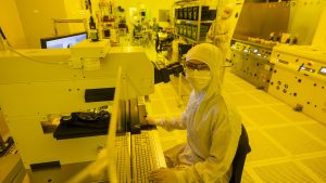
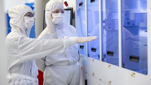
New investment in VTT’s cleanroom facility
The new equipment and processing capacity will be based at VTT’s Micronova facility and the planned Kvantinova hub in Otaniemi, Espoo. New capabilities are at the heart of the development of specialized chips for data storage and transfer applications, including new memory technologies, RF, piezo MEMS, integrated photonics, integrated technologies and superconducting quantum technologies, among others.
Enterprises and the broader ecosystem will have access to both new and upgraded processing capabilities, as well as existing VTT processing via VTT services in shared Micronova cleanrooms. These investments will enable companies to develop new products and services, boosting Finland’s growth. At the same time, Finnish companies will have access to European pilot line technology through VTT, further strengthening Finland’s processing capabilities, including those related to European processor technology.
Finland’s participation in the pilot line of European Chips JU microelectronics
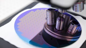
With the JU pilot line of microelectronic chips, VTT focuses on new processes and devices for specialized microelectronics. The FAMES pilot line is developing RF BAW filtering to support new communication bands up to 15 GHz. VTT also develops FeFET-based non-volatile memory technologies that are compatible with monolithic integration with CMOS, either as back-end or post-CMOS processing. Both technologies are combined with FD-SOI chips manufactured by LETI. In the APECS pilot line, VTT is developing integrated passive device (IPD) technology for RF integration. This technology is used in communications applications to support packaging and integration of BAW and RF transceivers. VTT is also focusing on RF technology with its NanoIC pilot line, evaluating the RF performance of 2nm CMOS technology developed by IMEC.
PIXEurope: Chips JU Photonics Pilot Line
Photonics is another field where Finland excels. Photonics Finland plays an important role in the development of the Finnish photonics ecosystem and has integrated photonics manufacturing technology at both VTT and the University of Tampere. The latter is involved in the Chips JU Wide Band Gap pilot line. With PIXEurope’s pilot line funding, VTT is investing in manufacturing capabilities and hybrid integration for more complex photonics chips. Combined with Tampere University’s expertise in compound semiconductors, this will enable a wide range of applications from communications to sensors. The Finnish Chip Competence Center (FiCCC) helps companies bring these new chip technologies to practical use.
In the PIXEurope pilot line, VTT is focusing on the further development of its 3µm thick SOI integrated photonics platform. VTT’s thick SOI PIC platform offers a combination of low optical loss, high density integration, and wide wavelength coverage. As part of the PIXEurope pilot line, VTT is investing in new equipment to process SOI wafers in its Micronova cleanroom to improve patterning resolution and surface smoothness of optical waveguide structures within PICs, as well as integrate other materials on SOI wafers to enable additional functionality such as high-speed optical modulation and optical detection.
european quantum pilot
Finland has a long tradition of research and development in superconducting quantum technology and is now home to world market leaders in this field.
However, quantum chip processing is still in its infancy and requires continued development to achieve reproducibility and reliability. The European Quantum Pilot is being launched for this purpose. VTT coordinates the European superconducting quantum technology pilot SUPREME and participates in other quantum pilots, putting Finland at the forefront of global quantum technology development.
With the increasing importance of quantum technology for new chips and applications, Finland’s involvement in the European Pilot Line is an important national investment, reinforcing its reputation as a pioneer in specialized microelectronics and Pilot Line activities. This participation will integrate Finland into the European chip supply chain, unlock new business and growth prospects for Finnish companies, and support the competitiveness and growth of the national economy. Additionally, SUPREME’s leadership has made Finland an important European technology development center.
In the SUPREME pilot, VTT will develop a scalable manufacturing process for superconducting quantum chips and Josephson junctions, which are key components of superconducting quantum systems. Development involves four different types of processes.
Angular evaporation bonding provides the best coherence bonding, but processing reproducibility requires improvement. Although the three-layer junction offers good reproducibility in manufacturing, improved coherence time is targeted. Superconducting 3D integration processes, including TSV and flip chips, enable the construction of multichip modules with superconducting interfaces and integration. The hybrid process supports the integration of RF and optics through superconducting nanowire single photon detectors (SNSPDs).
Complementing the strengths of the Nordic countries
Finland’s contribution to the European chip ecosystem is growing, strongly driven by VTT’s central position in the European pilot line ecosystem. Looking beyond Finland, the Nordic countries are well positioned to become major players in microelectronics, photonics and quantum technologies.
Together, these can make a significant contribution to Europe’s self-sufficiency and competitiveness in key technologies. The Nordic countries’ strengths are complemented by a deep research tradition, high-quality education and strong public-private cooperation. Leveraging these complementarities and expanding our collective innovation and impact is essential for further growth.
It is important for the Nordic countries to work together in the development and deployment of new and important technologies, enabling Nordic businesses and economies to grow with new opportunities.
author
Piia Konstari, VTT Microfabrication Services Director
Pekka Pursula, VTT Microelectronics and Quantum Research Director
This article will also be published in the quarterly magazine issue 24.
Source link